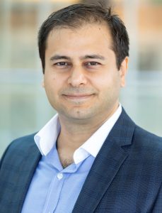
 Dr. Can Bayram is the Intel Alumni Endowed Faculty Scholar and an Associate Professor in the Department of Electrical and Computer Engineering and a resident faculty at the Nick Holonyak, Jr Micro and Nanotechnology Laboratory, University of Illinois at Urbana-Champaign, IL, USA.
The 21st century is the age of semiconductors. In all aspects of modern life, we utilize semiconductor technologies. From lighting to communication and computing to transportation, we rely on semiconductors for comfort, safety, and sustainability. Today, we are switching to solid-state lighting for halving our lighting electricity usage, 5G communication for networked devices, and autonomous systems for land/sea/air transportation. Our reliance on semiconductors is only to evolve as solid-state lighting extends into horticulture and medicine, new communication spectra above 95 gigahertz open opportunities for 6G and beyond networking, and space exploration leads to space settlements. Prof. Bayram understands, controls, and exploits semiconductor technologies and creates an innovative research and education platform considering the needs of not only the current but also of the next generation.
Prof. Bayram is the recipient of the International Union of Pure and Applied Physics Young Scientist Medal, the IEEE Nanotechnology Council Early Career Award, an NSF CAREER Award, a CS Mantech Best Paper Award, an AFOSR Young Investigator Award, the IEEE Electron Devices Society Early Career Award, and a Best Paper Award at the 11th International Conference on Infrared Optoelectronics. For his achievements in ultraviolet-to-terahertz engineering of III-V semiconductor materials and devices, OSA, SPIE, and IEEE recognized him with senior member status.
Prof. Bayram supervised(supervising) 4(4) Ph.D. theses, 2(0) M.S. thesis, 6(1) senior theses, 1(0) postdoctoral research scientist, and (co-) authored 62 journal papers (h-index ≥ 29), 42 conference proceeding papers, 4 book chapters, and has ≥ 52 patents issued/pending.
Select Honors
 |
COLLEGE-WIDE RECOGNITION Dean’s Award for Excellence in Research for Associate Professor (awarded to 6 associate professors amongst the eligible pool of 130+ (tenure-track) College of Engineering assistant professors, judged by the best research during the last five years) |
 |
NATION-WIDE RECOGNITION Invitation to the National Inventors Hall of Fame Collegiate Inventors Competition Final (Team Cubic LEDs, awarded to only five graduate-advisor teams nationally) |
 |
National Academy of Engineering Recognition Invitation to the China-America Frontiers of Engineering Symposium (CAFOE), hosted by Qualcomm and organized by the National Academy of Engineering (NAE) and Chinese Academy of Engineering (CAE). (held biennially, sixty participants – including the organizing committee and speakers – from Chinese and US universities, industry, and government are to cover four topics – Smart Cities, New Materials, Neuroengineering, and 5G Wireless Communication Technology during the two and a half days of the symposium) |
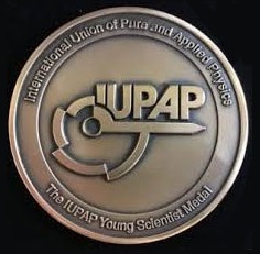 |
WORLD-WIDE RECOGNITION Young Scientist Medal (awarded annually to one in the world by the International Union of Pure and Applied Physics (IUPAP)) |
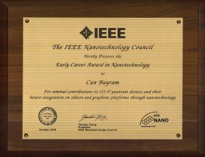 |
WORLD-WIDE RECOGNITION IEEE Nanotechnology Council Early Career Award (awarded annually to one in the world by the IEEE Nanotechnology Council) |
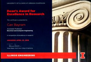 |
COLLEGE-WIDE RECOGNITION Dean’s Award for Excellence in Research for Assistant Professor (awarded to 6 assistant professors amongst the eligible pool of 135+ (tenure-track) College of Engineering assistant professors, judged by the best research during the last academic year) |
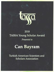 |
Turkish American Scientists & Scholars Association Recognition Turkish American Scientists & Scholars Association (TASSA) Young Scholar Award in recognition of his accomplishments as a young Turkish American scholar (two junior Turkish-American faculty is recognized every other year) |
 |
NATION-WIDE RECOGNITION NSF CAREER Award (awarded to 156 scientists amongst > 3,050 applicants (success rate of ~5%) in the U.S. by the National Science Foundation) |
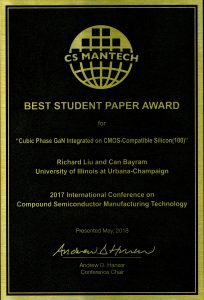 |
International Conference on Compound Semiconductor Manufacturing Technology Recognition CS MANTECH Best Student Paper Award (Mr. Richard (Dicky) Liu) at the 2017 International Conference on Compound Semiconductor Manufacturing Technology (CS MANTECH) (awarded to only 1 amongst 22 student presenters (success rate of < 5%)) |
 |
NATION-WIDE RECOGNITION AFOSR Young Investigator Award (awarded to 56 scientists amongst > 265 applicants (success rate of ~20%) in the U.S. by the Air Force Office of Scientific Research) |
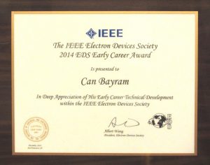 |
WORLD-WIDE RECOGNITION IEEE Electron Devices Society Early Career Award (awarded annually to one in the world by the IEEE Electron Devices Society) |
 |
OSA Society Recognition OSA Society Senior Membership in recognition of his experience and professional accomplishments in the field of optics and photonics. |
 |
IEEE Society Recognition IEEE Society Senior Membership elevation (awarded to only 9% of IEEE’s approximately 428,000 members) for significant technical accomplishments in GaN devices and for significant contributions as an educator in the field of electronics, optics, and photonics. |
 |
SPIE Society Recognition SPIE Society Senior Membership elevation for significant technical accomplishments in GaN devices and for significant contributions as an educator in the field of optics and photonics. |
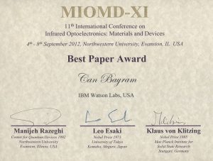 |
11th International Conference on Infrared Optoelectronics: Materials and Devices Recognition Best Paper Award at the Infrared Optoelectronics Materials and Devices Conference, MIOMD-XI, that was co-chaired by Franklin Medal Laureate Prof. Manijeh Razeghi, Nobel Laureate Prof. Leo Esaki and Nobel Laureate Prof. Klaus von Klitzing) |
 |
WORLD-WIDE RECOGNITION IBM Ph.D. Fellowship (awarded annually to select researchers in the world by the International Business Machines Corporation) |
 |
USA & CANADA RECOGNITION Link Foundation Energy Fellowship (awarded annually to three in USA and Canada by the Link Foundation) |
 |
WORLD-WIDE RECOGNITION Boeing Engineering Student of the Year (awarded annually to one in the world by the Boeing Company) |
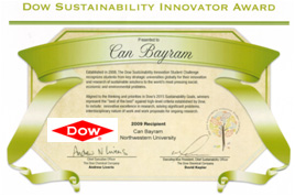 |
WORLD-WIDE RECOGNITION Dow Sustainability Innovation Award (awarded to one in select worldwide universities by the Dow Chemical Company) |
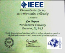 |
WORLD-WIDE RECOGNITION IEEE Electron Devices Society PhD Fellowship (awarded to three in the world – one in USA – by the IEEE Electron Devices Society) |
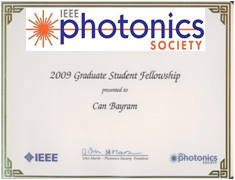 |
WORLD-WIDE RECOGNITION IEEE Photonics Society Graduate Student Fellowship (awarded to twelve in the world – seven in USA – by the IEEE Photonics Society) |
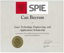 |
WORLD-WIDE RECOGNITION SPIE Laser Technology, Engineering and Applications Scholarship (awarded to one in the world – third top recognition – by the SPIE Society) |
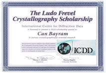 |
WORLD-WIDE RECOGNITION Ludo Frevel Crystallography Scholarship (awarded to ten in the world by the International Centre for Diffraction Data (ICDD)) |
 |
IEEE Ultrasonics Symposium Recognition Travel Award (awarded to select by the IEEE Ultrasonics, Ferroelectrics, and Frequency Control Society) |