| (24) | 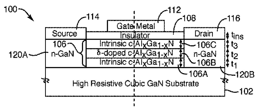 |
C. Bayram, J. O. Chu, C. Dimitrakopoulos, J. Kim, H. Park, and D.K. Sadana, “Thin film wafer transfer and structure for electronic devices,” U.S. Patent 10,957,816 (issued March 23, 2021). link or pdf
|
| (23) | |
C. Bayram, R.W. Grady, and K. Park, “Normally-off cubic phase GaN (c-GaN) HEMT having a gate electrode dielectrically insulated from a c-AlGaN capping layer,” U.S. Patent 10,211,328 (issued February 19, 2019). link or pdf
|
| (22) |  |
C. Bayram, C.P. D’Emic, J. Kim, and D.K. Sadana, “Hetero-integration of III-N material on silicon,” U.S. Patent 10,056,251 (issued August 21, 2018). link or pdf
|
| (21) |  |
C. Bayram and R. Liu, “Maximizing cubic phase group III-nitride on patterned silicon,” U.S. Patent 10,027,086 (issued July 17, 2018). link or pdf
|
| (20) |  |
C. Bayram, S. W. Bedell, N. Li, K.T. Shiu, and D. K. Sadana, “Back contact LED through spalling,” U.S. Patent 9,865,769 (issued January 9, 2018). link or pdf
|
| (19) |  |
C. Bayram, C.P. D’Emic, W.J. Gallagher, E. Leobandung, and D.K. Sadana, “Group III nitride integration with CMOS technology,” U.S. Patent 9,660,069 (issued May 23, 2017). link or pdf
|
| (18) |  |
C. Bayram, C.-W. Cheng, T. Gokmen, N. Li, J.A. Ott, K.T. Shiu, and D.K. Sadana, , “Polarization free gallium nitride-based photonic devices on nanopatterned silicon,” |
| (17) |  |
C. Bayram, C.P. D’Emic, J. Kim, and D.K. Sadana, “Hetero-integration of III-N material on silicon,” U.S. Patent 9,601,583 (issued March 21, 2017). link or pdf
|
| (16) |  |
C. Bayram, C. Dimitrakopoulos, K. Fogel, J. Kim, J.A. Ott, and D.K. Sadana, “Gallium nitride material and device deposition on graphene terminated wafer and method of forming the same,” U.S. Patent 9,574,287 (issued February 21, 2017). link or pdf |
| (15) |  |
C. Bayram, C.P. D’Emic, W.J. Gallagher, E. Leobandung, and D.K. Sadana, “Group III nitride integration with CMOS technology,” U.S. Patent 9,564,526 (issued February 7, 2017). link or pdf |
| (14) |  |
C. Bayram, C.-W. Cheng, D.K. Sadana, and K.-T. Shiu, “Selective gallium nitride regrowth on (100) silicon,” |
| (13) |  |
C. Bayram, C.P. D’Emic, W.J. Gallagher, E. Leobandung, and D.K. Sadana, “Group III nitride integration with CMOS technology,” |
| (12) |  |
C. Bayram, C.P. D’Emic, W.J. Gallagher, E. Leobandung, and D.K. Sadana, “Group III nitride integration with CMOS technology,” |
| (11) |  |
C. Bayram, S. W. Bedell, and D. K. Sadana, “Engineered base substrates for releasing III-V epitaxy through spalling,” U.S. Patent 9,245,747 (issued January 26, 2016). link or pdf |
| (10) |  |
C. Bayram, S. W. Bedell, D. K. Sadana, and K. L. Saenger, “Laser-initiated exfoliation of group iii-nitride films and applications for layer transfer and patterning,” U.S. Patent 9,236,271 (issued January 12, 2016). link or pdf |
| (9) |  |
C. Bayram, C.-W. Cheng, T. H. Ning, D.K. Sadana, and K.-T. Shiu, “Heterogeneous integration of group III nitride on silicon for advanced integrated circuits ,” U.S. Patent 9,236,251 (issued January 12, 2016). link or pdf |
| (8) |  |
C. Bayram, C.-W. Cheng, D.K. Sadana, and K.-T. Shiu, “Selective gallium nitride regrowth on (100) silicon,” |
| (7) |  |
C. Bayram, C.-W. Cheng, D.K. Sadana, and K.-T. Shiu, “Selective gallium nitride regrowth on (100) silicon ,” U.S. Patent 9,059,075 (issued June 16, 2015). link or pdf
|
| (6) |  |
C. Bayram and D.K. Sadana, “Light emitting diodes with via contact scheme ,” U.S. Patent 9,059,339 (issued June 16, 2015). link or pdf
|
| (5) |  |
C. Bayram, S.W. Bedell, K.E. Fogel, J. A. Ott, and D.K. Sadana, “Controlled spalling of group III nitrides containing an embedded spall releasing plane ,” |
| (4) |  |
C. Bayram, C.-W. Cheng, T. H. Ning, D.K. Sadana, and K.-T. Shiu, “Heterogeneous integration of group III nitride on silicon for advanced integrated circuits ,” U.S. Patent 9,053,930 (issued June 9, 2015). link or pdf
|
| (3) |  |
C. Bayram, C.-W. Cheng, D.K. Sadana, and K.-T. Shiu, “Dual phase gallium nitride material formation on (100) silicon ,” |
| (2) |  |
C. Bayram, D.K. Sadana, and K.-T. Shiu, “Group III nitrides on nanopatterned substrates,” U.S. Patent 8,927,398 (issued January 6, 2015). link or pdf
|
| (1) |  |
C. Bayram, J. O. Chu, C. Dimitrakopoulos, J. Kim, H. Park, and D.K. Sadana, “Thin film wafer transfer and structure for electronic devices,” U.S. Patent 8,916,451 (issued December 23, 2014). link or pdf |