| (62) | 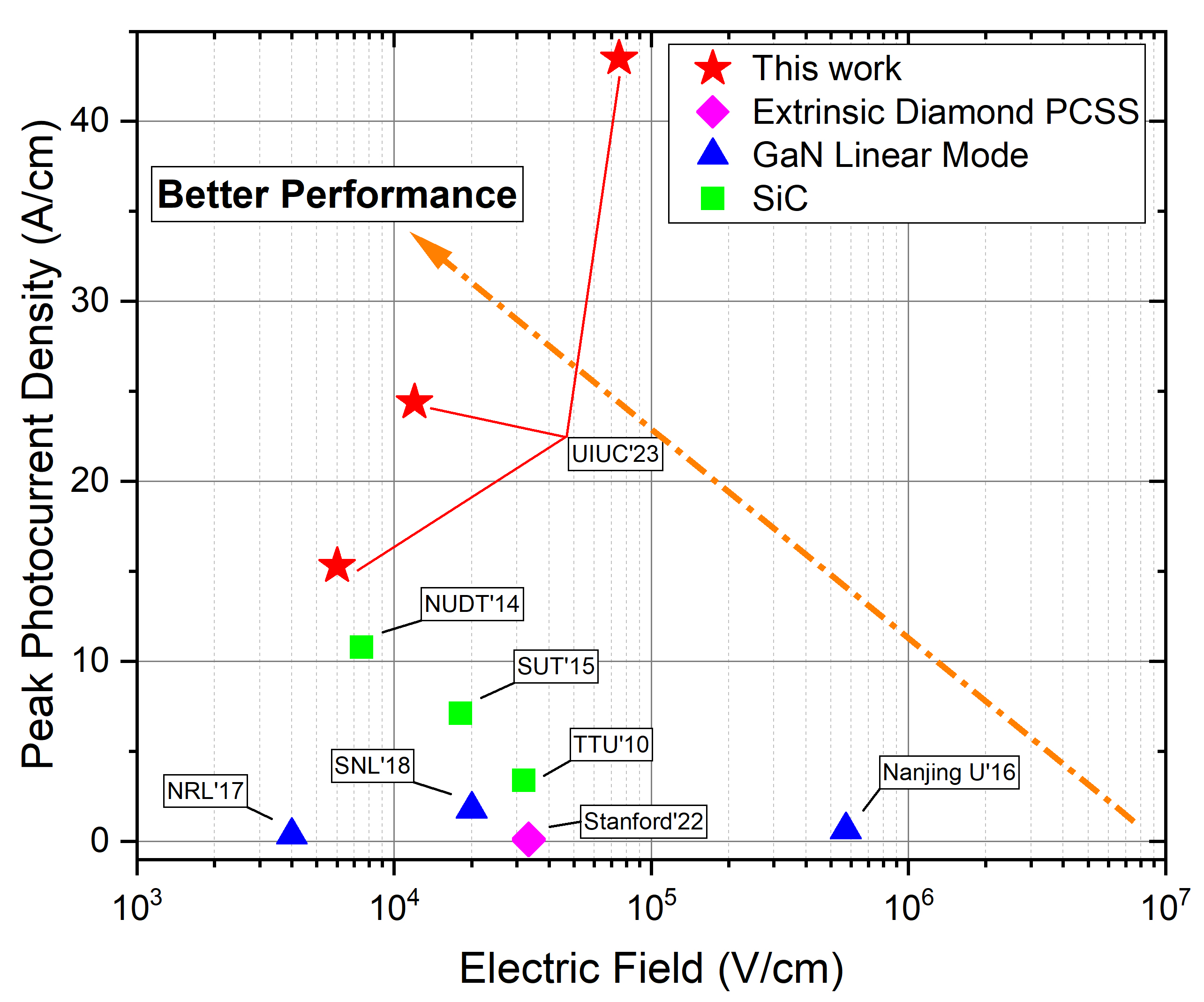 |
Z. Han, J. Lee, S. Messing, T. Reboli, A. Mironov, and C. Bayram,
“Buried Channel Diamond Photoconductive Switch with High Above-Bandgap Responsivity,” IEEE Electron Device Lett. (2024). link |
| (61) | 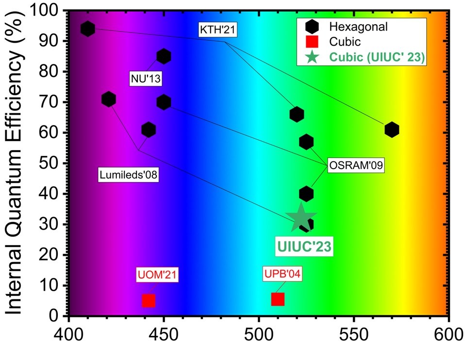 |
(EDITOR’S PICK) (FRONT COVER ARTICLE)J. Lee and C. Bayram,
“Green-emitting Cubic GaN/In0.16Ga0.84N/GaN Quantum Well with 32% Internal Quantum Efficiency at Room Temperature,” Appl. Phys. Lett. 124, 011101 (2024). link |
| (60) | 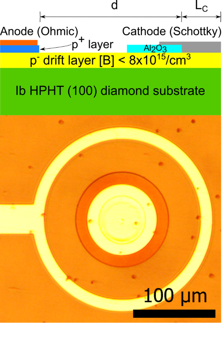 |
(TOP Downloaded Article)Z. Han and C. Bayram,
“Diamond p-type lateral Schottky barrier diodes with high breakdown voltage (4612 V at 0.01 mA/mm),” IEEE Electron Device Lett. 44 (10) 1692 (2023). link |
| (59) | 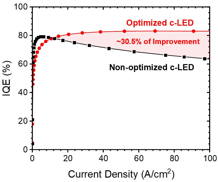 |
(EDITOR’S PICK) (TOP Downloaded Article)J. Lee, J.P. Leburton, and C. Bayram,
“Design trade-offs between traditional hexagonal and emerging cubic InXGa(1-X)N/GaN-based green light-emitting diodes,” J. Opt. Soc. Am. B 40(5), 1017-1023 (2023). link |
| (58) | 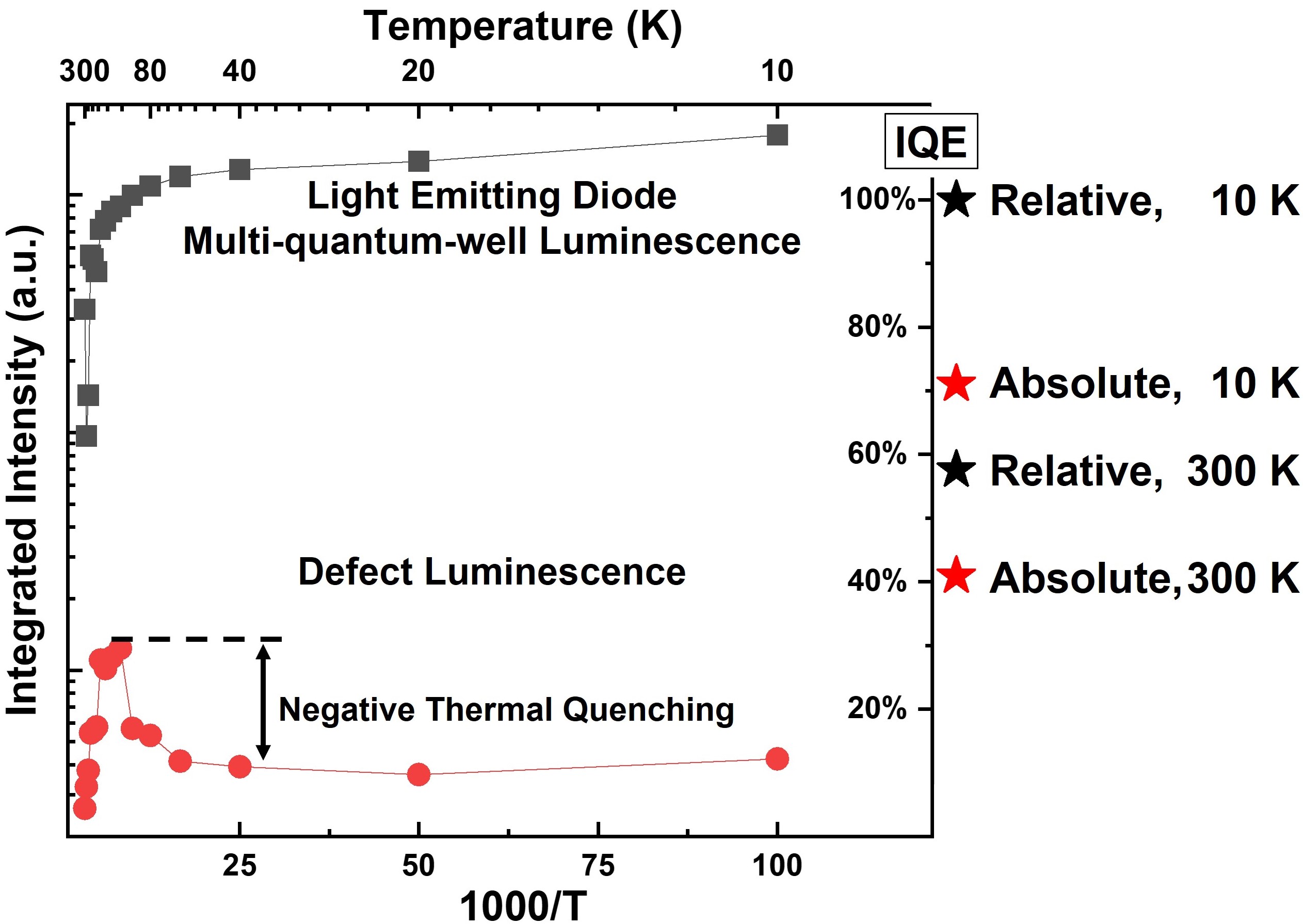 |
Y. C. Chiu and C. Bayram,
“Low Temperature Absolute Internal Quantum Efficiency of InGaN-based Light-Emitting Diodes,” Appl. Phys. Lett. 122, 091101 (2023). link |
| (57) | 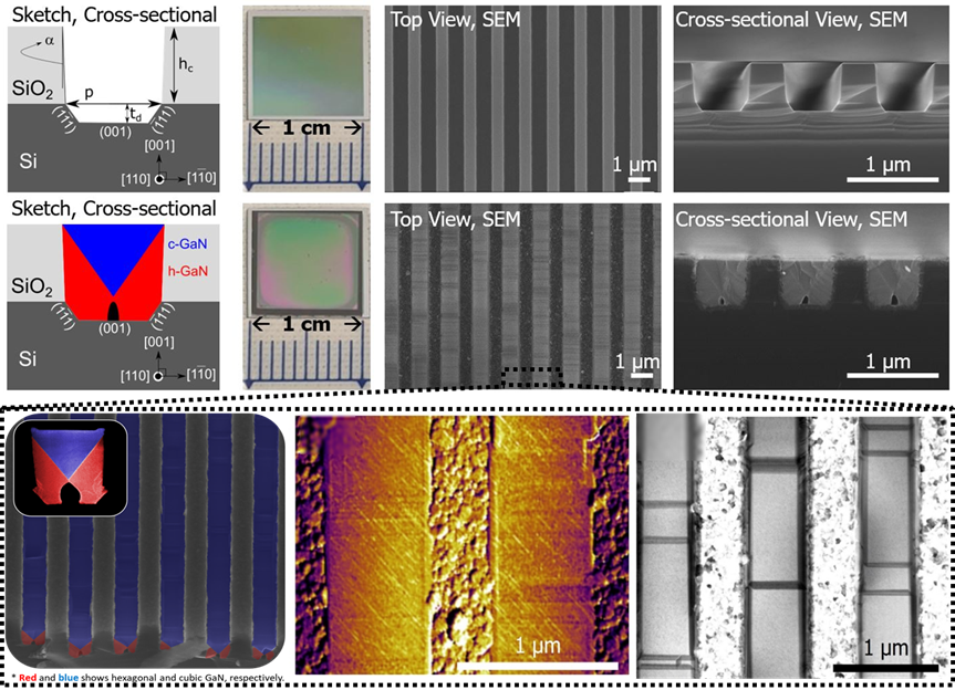 |
(EDITOR’S PICK)
J. Lee*, Y. C. Chiu*, M. A. Johar*, and C. Bayram, “Structural and Optical Properties of Cubic GaN on U-grooved Si (100),” Appl. Phys. Lett. 121, 032101 (2022). link |
| (56) | 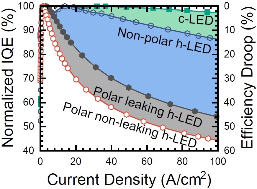 |
Y.-C. Tsai, C. Bayram, and J.P. Leburton, “Interplay between Auger recombination, Carrier Leakage, and Polarization in InGaAlN Multiple-Quantum-Well Light-Emitting Diodes,” J. Appl. Phys. 131, 193102 (2022). link |
| (55) | 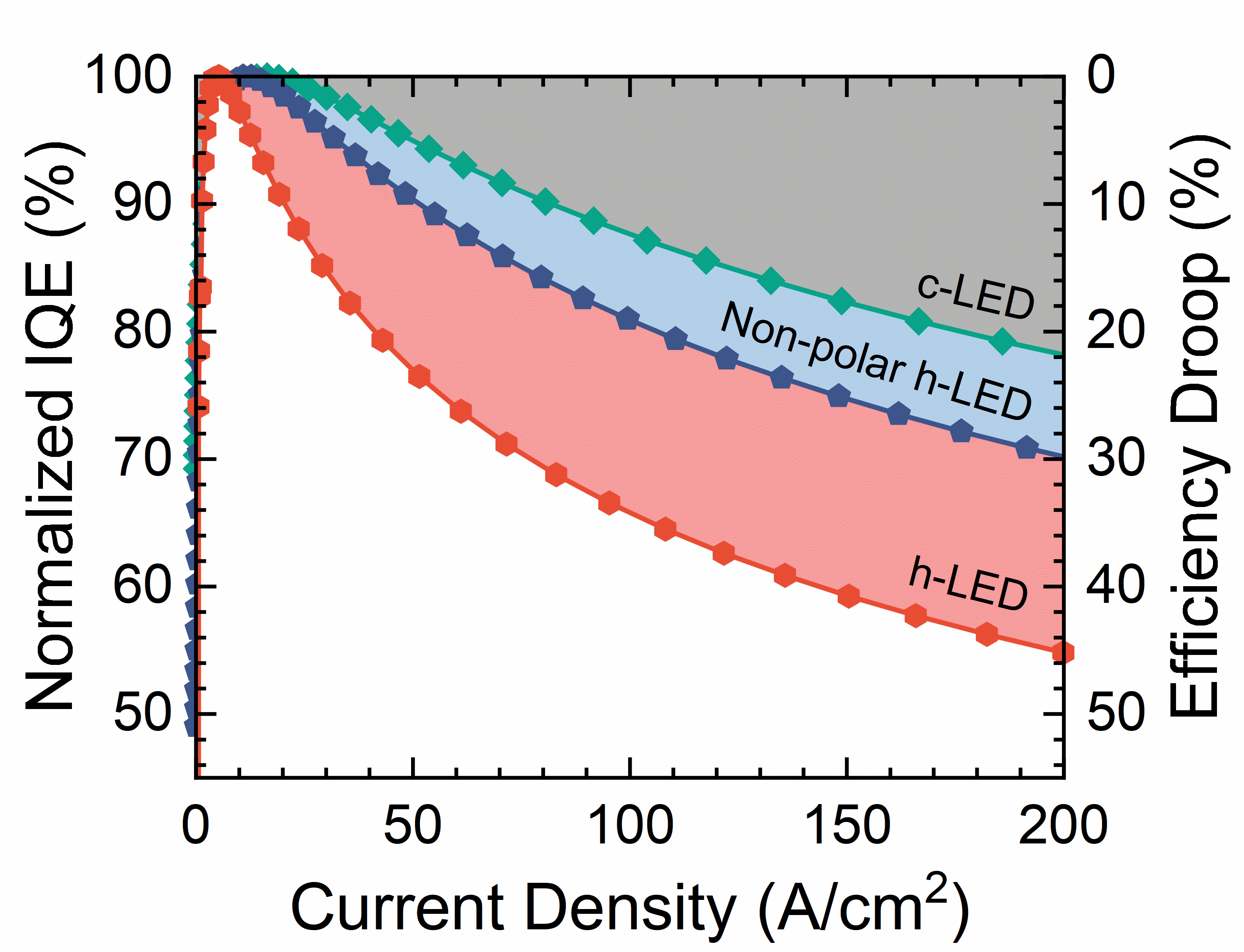 |
Y.-C. Tsai, J.P. Leburton, C. Bayram, “Quenching of the Efficiency Droop in Cubic Phase InGaAlN Light-Emitting Diodes,” IEEE Trans. Electron Devices 69(6), 3240-3245 (2022). link |
| (54) | 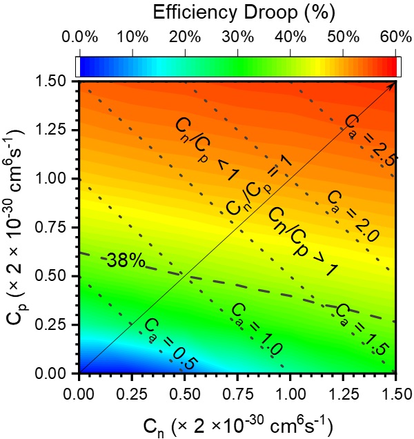 |
Y.-C. Tsai, C. Bayram, and J.P. Leburton, “Effect of Auger Electron–Hole Asymmetry on the Efficiency Droop in InGaN Quantum Well Light-Emitting Diodes,” IEEE J. Quantum Electron. 58 (1), 1-9 (2022). link |
| (53) | 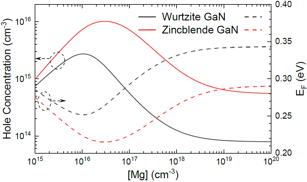 |
Y.-C. Tsai and C. Bayram, “Mitigate Self-Compensation with High Crystal Symmetry: A First–Principles Study of Formation and Activation of Impurities in GaN,” Comp. Mater. Sci. 190, 110283 (2021). link |
| (52) | 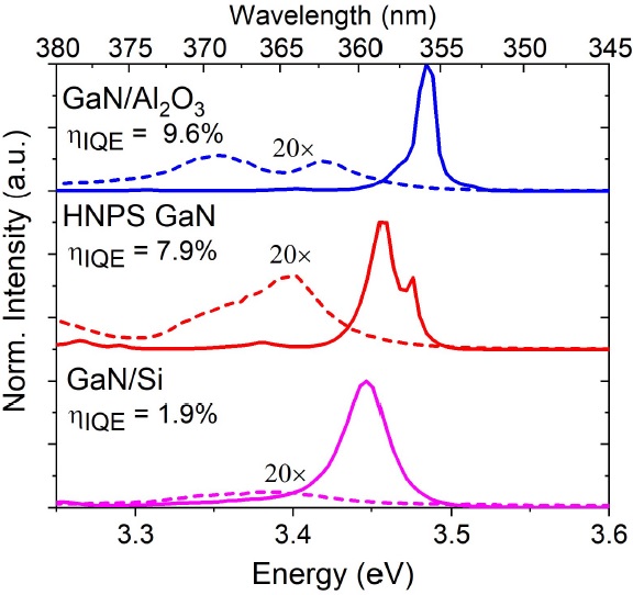 |
J. Meyer, R. Liu, R.D. Schaller, H-P Lee, and C. Bayram, “Systematic Study of Shockley-Read-Hall and Radiative Recombination in GaN on Al2O3, Freestanding GaN, and GaN on Si,” J. Phys. Photonics 2, 035003 (2020). link |
| (51) | 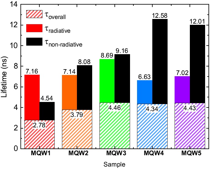 |
R. Liu, E. Z. Tucker, S. M. Lee, K. Kasarla, C. McCormick, and C. Bayram, “Cp2Mg-Induced Transition Metal Ion Contamination and Performance Loss in MOCVD-Grown Blue Emitting InGaN/GaN Multiple Quantum Wells,” Appl. Phys. Lett. 116, 192106 (2020). link |
| (50) |  |
A. Mohamed, K. Park, C. Bayram, M. Dutta, and M. Stroscio, “Phonon-assisted reduction of hot spot temperature in AlInN ternaries,” J. Phys. D-Appl. Phys. 53, 365102 (2020). link |
| (49) |  |
H-P Lee and C. Bayram, “Improving Current on/off Ratio and Subthreshold Swing of Schottky-gate AlGaN/GaN HEMTs By Post-metallization Annealing,” IEEE Trans. Electron Devices 67 (7), 2760 (2020). link |
| (48) |  |
(FRONT COVER ARTICLE)
Y.-C. Tsai and C. Bayram, “Band Alignments of Ternary Wurtzite and Zincblende III-Nitrides Investigated by Hybrid Density–Functional Theory,” ACS Omega 5, 3917 – 3923 (2020). link |
| (47) |  |
K. Park and C. Bayram, “Impact of dislocations on the thermal conductivity of gallium nitride studied by time-domain thermoreflectance,” J. Appl. Phys. 126, 185103 (2019). link |
| (46) |  |
H-P Lee and C. Bayram, “Investigation of annealed, thin(~ 2.6 nm)-Al2O3/AlGaN/GaN metal-insulator-semiconductor heterostructures on Si(111) via capacitance-voltage and current-voltage studies,” Mater. Res. Express 6, 105904 (2019). link |
| (45) |  |
Y.-C. Tsai and C. Bayram, “Structural and Electronic Properties of Hexagonal and Cubic Phase AlGaInN Alloys Investigated Using First Principles Calculations,” Sci. Rep. 9:6583 (2019). link |
| (44) |  |
A. Mohamed, K. Park, C. Bayram, M. Dutta, and M. Stroscio, “Confined and Interface Optical Phonon Emission in GaN/InGaN Double Barrier Quantum Well Heterostructures,” PLoS One 14(4): e0214971 (2019). link |
| (43) | 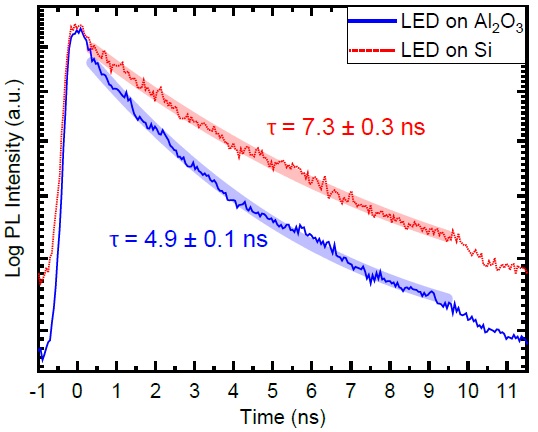 |
R. Liu, C. McCormick, and C. Bayram, “Comparison of Structural and Optical Properties of Blue Emitting In0.15Ga0.85N/GaN Multi-Quantum-Well Layers Grown on Sapphire and Silicon Substrates,” AIP Advances 9, 025306 (2019). link |
| (42) | 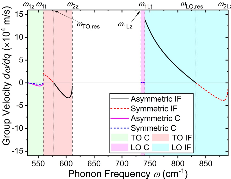 |
K. Park, A. Mohamed, M. Dutta, M. Stroscio, and C. Bayram, “Electron Scattering via Interface Optical Phonons with High Group Velocity in Wurtzite GaN-based Quantum Well Heterostructure,” Sci. Rep. 8:15947 (2018). link |
| (41) | 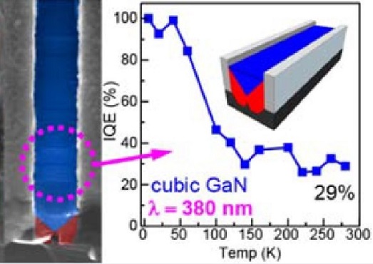 |
R. Liu, R. Schaller, C.-Q. Chen, and C. Bayram, “High internal quantum efficiency ultraviolet emission from phase-transition cubic GaN integrated on nanopatterned Si(100),” ACS Photonics 5 (3), 955–963 (2018). link |
| (40) | 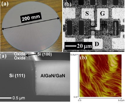 |
K.-T. Lee, C. Bayram, D. Piedra, E. Sprogis, H. Deligianni, B. Krishnan, G. Papasouliotis, A. Paranjpe, E. Aklimi, K. Shepard, W. J. Gallagher, T. Palacios, and D. K. Sadana, “Heterogeneous Integration of GaN Devices on a 200 mm Si(100) Wafer via Scalable CMOS Technology,” IEEE Electron Device Lett. 38 (8) 1094 – 1096 (2017). link |
| (39) |  |
K. Park, M. A. Stroscio, and C. Bayram, “Investigation of electron mobility and saturation velocity limits in gallium nitride using uniaxial dielectric continuum model,” J. Appl. Phys. 121, 245109 (2017). link |
| (38) |  |
R. Grady and C. Bayram, “Simulation of zincblende AlGaN/GaN high electron mobility transistors for normally-off operation,” J. Phys. D: Appl. Phys. 50, 265104 (2017). link |
| (37) |  |
J. Perozek, H.-P. Lee, B. Krishnan, G. Papasouliotis, A. Paranjpe, K. B. Reuter, D. K. Sadana, and C. Bayram, “Investigation of Structural, Optical, and Electrical Characteristics of an AlGaN/GaN High Electron Mobility Transistor Structure across a 200 mm Si (111) Substrate,” J. Phys. D: Appl. Phys. 50, 055103 (2017). link |
| (36) |  |
H-P Lee, J. Perozek, L. N. D. Rosario, and C. Bayram, “Investigation of AlGaN/GaN high electron mobility transistor structures on 200-mm silicon (111) substrates employing different buffer layer configurations,” Sci. Rep. 6: 37588 (2016). link |
| (35) | 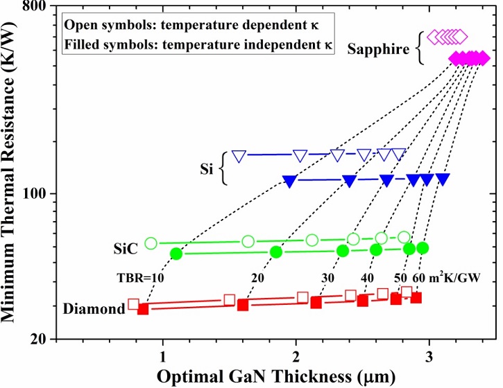 |
K. Park and C. Bayram, “Thermal Resistance Optimization of GaN / Substrate Stacks Considering Thermal Boundary Resistance and Temperature-dependent Thermal Conductivity,” Appl. Phys. Lett. 109, 151904 (2016). link |
| (34) |  |
R. Liu and C. Bayram, “Maximizing Cubic Phase Gallium Nitride Surface Coverage on Nano-patterned Silicon (100),” Appl. Phys. Lett. 109, 042103 (2016). link |
| (33) |  |
R. Liu and C. Bayram, “Cathodoluminescence study of luminescence centers in hexagonal and cubic phase GaN hetero-integrated on Si(100),” J. Appl. Phys. 120, 025106 (2016). link |
| (32) |  |
J. Kim† & C. Bayram†(† equal contribution), H. Park, C.-W. Cheng,C. Dimitrakopoulos, J. A. Ott, K. B. Reuter, S. W. Bedell, and D.K. Sadana, “Principle of direct van der Waals epitaxy of single-crystalline films on epitaxial graphene,” Nat. Comm. 5: 4836 (2014). link |
| (31) |  |
(FRONTISPIECE ARTICLE) C. Bayram, J. Ott, K.-T. Shiu, C.-W. Cheng, Y. Zhu, J. Kim, M. Razeghi, and D.K. Sadana, “Cubic Phase GaN on Nano-grooved Si (100) via Maskless Selective Area Epitaxy,” Adv. Funct. Mater. 24 (28) 4492 (2014). link |
| (30) | 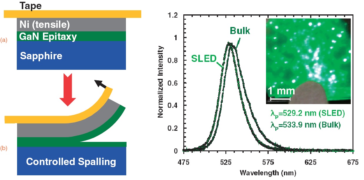 |
S. W. Bedell, C. Bayram, K. Fogel, P. Lauro, J. Kiser, J. Ott, Y. Zhu, and D. Sadana, “Vertical Light-Emitting Diode Fabrication by Controlled Spalling,” Appl. Phys. Express 6 (11), 112301 (2013). link |
| (29) |  |
(INSIDE COVER ARTICLE) D. Shahrjerdi, S. W. Bedell, C.Bayram, C. C. Lubguban, K. Fogel, P. Lauro, J. A. Ott, M. Hopstaken, M. Gayeness, and D. Sadana, “Ultra-Light High-Efficiency Flexible InGaP/(In)GaAs Tandem Solar Cells on Plastic,” Adv. Energy Mater. 3 (5), 566–571 (2013). link |
| (28) |  |
Y. Zhang, S. Gautier, C.-Y. Cho, E. Cicek, Z. Vashaei, R. McClintock, C. Bayram, Y. Bai, and M. Razeghi, “Near Miliwatt Power AlGaN-based Ultraviolet Light Emitting Diodes based on Lateral Epitaxial Overgrowth of AlN on Si(111),” Appl. Phys. Lett. 102, 011106 (2013). link |
| (27) | 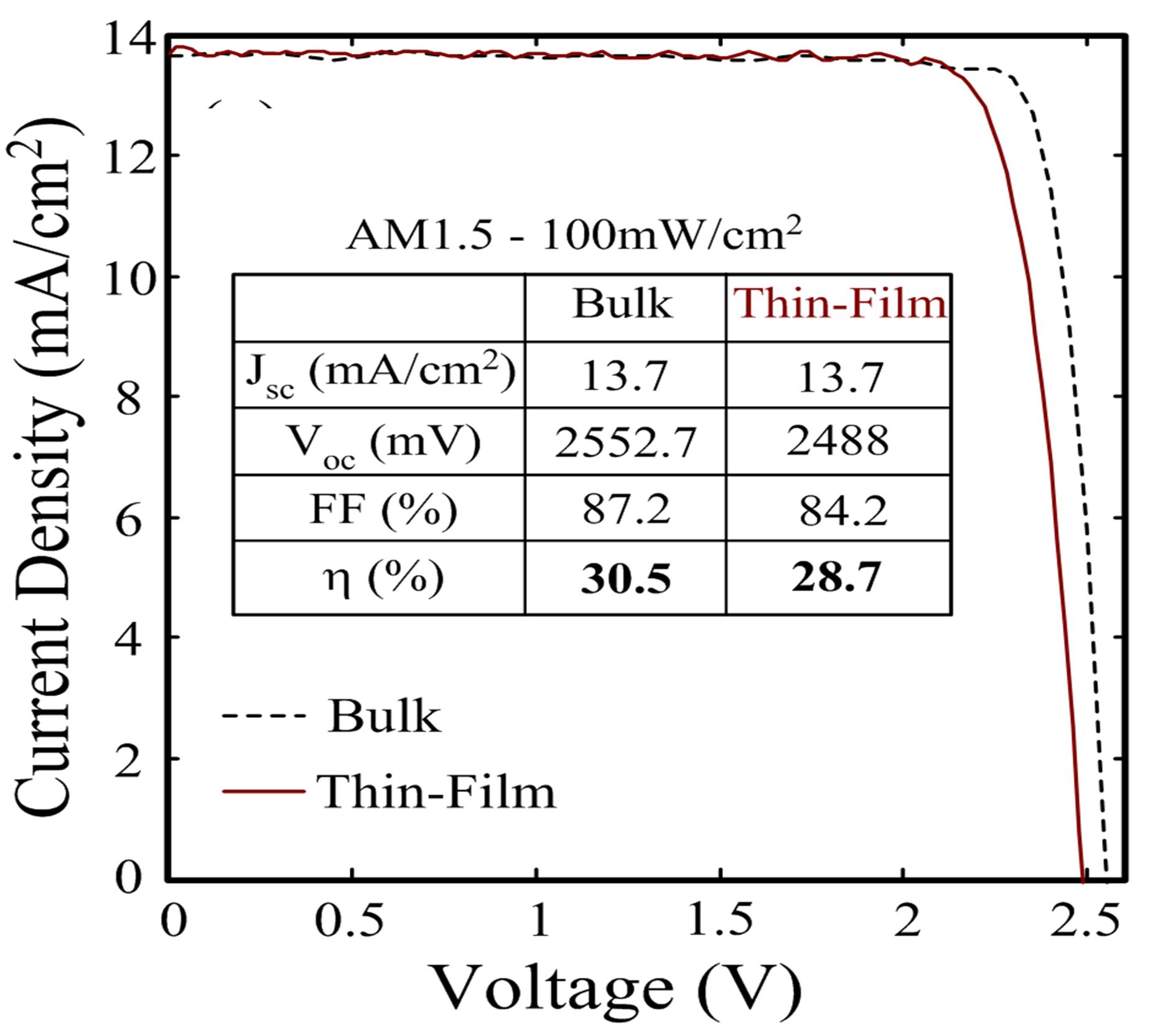 |
(EDITOR’S CHOICE 2012) (APL TOP 20 MOST DOWNLOADED) D. Shahrjerdi, S. W. Bedell, C. Ebert, C. Bayram, B. Hekmatshoar, K. Fogel, P. Lauro, M. Gaynes, T. Gokmen, J. Ott, and D. K. Sadana, “High-Efficiency Thin-Film InGaP/InGaAs/Ge Tandem Solar Cells Enabled By Controlled Spalling Technology,” Appl. Phys. Lett. 100, 053901 (2012). link |
| (26) | 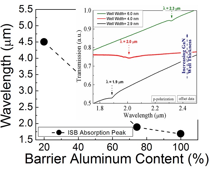 |
C. Bayram, “High quality AlGaN/GaN superlattices for near- and mid-infrared intersubband transitions,” J. Appl. Phys. 111, 013514 (2012). link |
| (25) |  |
C. Bayram, Z. Vashaei, and M. Razeghi, “Reliability in room-temperature negative differential resistance characteristics of low-aluminium-content AlGaN/GaN double-barrier resonant tunneling diodes,” Appl. Phys. Lett. 97, 181109 (2010). link |
| (24) | 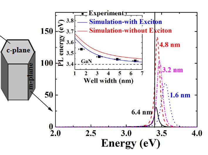 |
Z. Vashaei, C. Bayram, P. Lavenus, and M. Razeghi, “Photoluminescence characteristics of polar and nonpolar AlGaN/GaN superlattices,” Appl. Phys. Lett. 97, 121918 (2010). link |
| (23) | 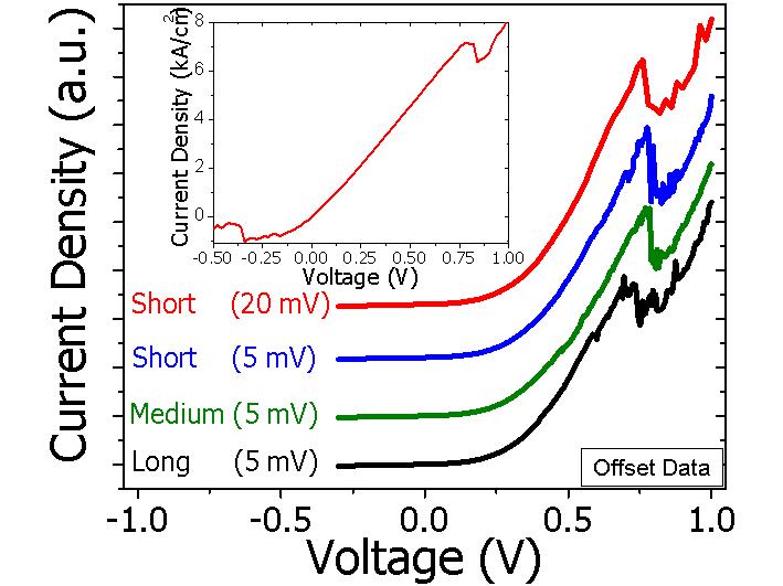 |
C. Bayram, Z. Vashaei, and M. Razeghi, “Room temperature negative differential resistance characteristics of polar III-nitride resonant tunneling diodes,” Appl. Phys. Lett. 97, 092104 (2010). link |
| (22) | 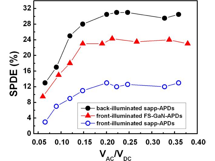 |
E. Cicek, Z. Vashaei, R. McClintock, C. Bayram, and M. Razeghi, “Geiger-mode operation of ultraviolet avalanche photodiodes grown on sapphire and free-standing GaN substrates,” Appl. Phys. Lett. 96, 261107 (2010). link |
| (21) |  |
Z. Vashaei, E. Cicek, C. Bayram, R. McClintock, and M. Razeghi, “GaN avalanche photodiodes grown on m-plane freestanding GaN substrate,” Appl. Phys. Lett. 96, 201908 (2010). link |
| (20) | 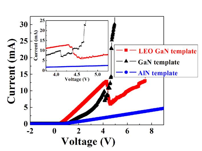 |
Z. Vashaei, C. Bayram and M. Razeghi, “Demonstration of negative differential resistance in GaN/AlN resonant tunneling diodes at room temperature,” J. Appl. Phys. 107, 083505 (2010). link |
| (19) |  |
C. Bayram, Z. Vashaei, and M. Razeghi, “AlN/GaN double-barrier resonant tunneling diodes grown by metal-organic chemical vapor deposition,” Appl. Phys. Lett. 96, 042103 (2010). link |
| (18) |  |
C. Bayram, N. Péré-Laperne, and M. Razeghi, “Effects of well width and growth temperature on optical and structural characteristics of AlN/GaN superlattices grown by metal-organic chemical vapor deposition,” Appl. Phys. Lett. 95, 201906 (2009). link |
| (17) |  |
N. Péré-Laperne, C. Bayram, L. Nguyen-Thê, R. McClintock, and M. Razeghi,“Tunability of Intersubband absorption from 4.5 to 5.3 µm in a GaN/Al0.2Ga0.8N superlattices grown by metalorganic chemical vapor deposition,”Appl. Phys. Lett. 95, 131109 (2009). link |
| (16) |  |
C. Bayram and M. Razeghi, “ULTRAVIOLET DETECTORS: Nitrides push performance of UV photodiodes,” Laser Focus World 45(9), 47-51 (2009). link |
| (15) | 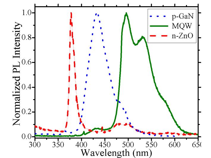 |
C. Bayram, D. Rogers, F. H. Teherani, and M. Razeghi, “Fabrication and Characterization of Novel Hybrid Green LEDs Based on Substituting n-type ZnO for n-type GaN in an Inverted p-n Junction,” J. Vac. Sci. Technol. B 27 (3), 1784 (2009). link |
| (14) |  |
V. E. Sandana, D. J. Rogers, F. H. Teherani, R. McClintock, C.Bayram, M. Razeghi, H.-J. Drouhin, M.C. Clochard, V. Sallet, G. Garry, and F. Falyouni, “Comparison of ZnO Nanostructures Grown Using pulsed layer deposition, metalorganic chemical vapor deposition, and physical vapor transport,” J. Vac. Sci. Technol. B 27 (3), 1678 (2009). link |
| (13) |  |
C. Bayram, N. Péré-laperne, R. McClintock, B. Fain and M. Razeghi, “Pulsed Metalorganic Chemical Vapor Deposition of High Quality AlN/GaN Superlattices for Near-Infrared Intersubband Transitions,” Appl. Phys. Lett. 94, 121902 (2009). link |
| (12) |  |
C. Bayram and M. Razeghi, “Stranski-Krastanov growth of InGaN quantum dots emitting in green spectra,” Appl. Phys. A – Mater. 96, 403 (2009). link |
| (11) |  |
C. Bayram, J. L. Pau, R. McClintock, and M. Razeghi, “Comprehensive study of blue and green multi-quantum-well light emitting diodes grown on conventional and lateral epitaxial overgrowth GaN,” Appl. Phys. B – Lasers Opt. 95, 307 (2009). link |
| (10) | 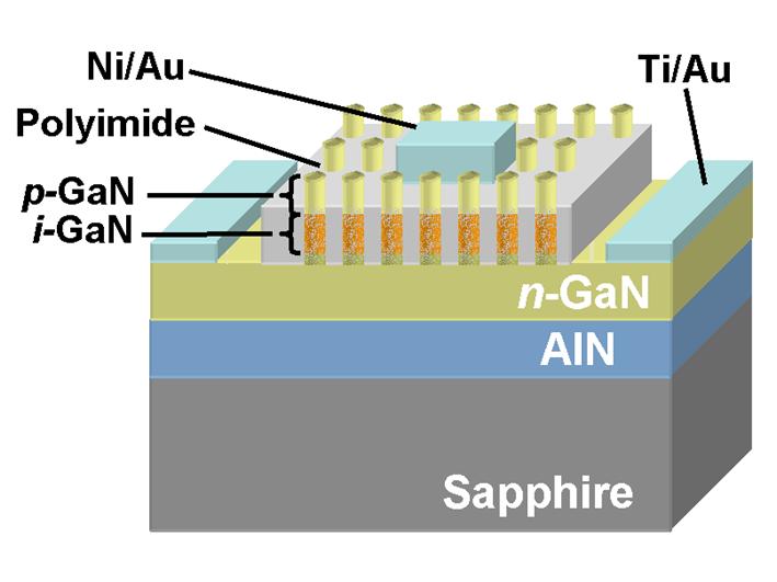 |
J. L. Pau, C. Bayram, P. Giedraitis, R. McClintock, and M. Razeghi, “GaN nanostructured p-i-n photodiodes,” Appl. Phys. Lett. 93, 221104 (2008). link |
| (9) | 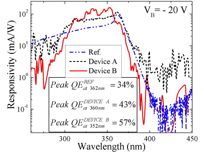 |
C. Bayram, J. L. Pau, R. McClintock, M. Razeghi, M. P. Ulmer, and D. Silversmith, “High Quantum Efficiency Back-illuminated GaN Avalanche Photodiodes,” Appl. Phys. Lett. 93, 211107 (2008). link |
| (8) |  |
(APL TOP 20 MOST DOWNLOADED) C. Bayram, F. H. Teherani, D. Rogers, and M. Razeghi, “A hybrid green light-emitting diode comprised of n-ZnO/(InGaN/GaN) multi-quantum wells/p-GaN,” Appl. Phys. Lett. 93, 081111 (2008). link |
| (7) | 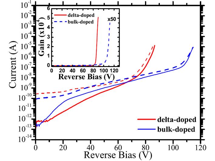 |
C. Bayram, J. L. Pau, R. McClintock, and M. Razeghi,“Performance enhancement of GaN ultraviolet avalanche photodiodes with p-type delta-doping,”Appl. Phys. Lett. 92, 241103 (2008). link |
| (6) | 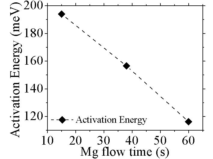 |
C. Bayram, J. L. Pau, R. McClintock, and M. Razeghi, “Delta-doping optimization for high quality p-type GaN,” J. Appl. Phys. 104, 083512 (2008). link |
| (5) |  |
J. L. Pau, C. Bayram, R. McClintock, D. Silversmith, and M. Razeghi, “Back-illuminated separate absorption and multiplication GaN avalanche photodiodes,” Appl. Phys. Lett. 92, 101120 (2008). link |
| (4) |  |
J. L. Pau, R. McClintock, C. Bayram, K. Minder, D. Silversmith, and M. Razeghi, “High Optical Response in Forward Biased (In,Ga)N-GaN MultiquantumWell Diodes under Barrier Illumination,” IEEE J. Quantum Elect. 44, 346 (2008). link |
| (3) |  |
K. Minder, J. L. Pau, R. McClintock, P. Kung, C. Bayram, M. Razeghi, and D. Silversmith, “Scaling in GaN avalanche photodiodes designed for back-illumination,” Appl. Phys. Lett. 91, 073513 (2007). link |
| (2) |  |
J. L. Pau, R. McClintock, K. Minder, C. Bayram, P. Kung, M. Razeghi, E. Munoz, and D. Silversmith, “Geiger-mode operation of back-illuminated GaN avalanche photodiodes,” Appl. Phys. Lett. 91, 041104 (2007). link |
| (1) |  |
R. McClintock, J. L. Pau, K. Minder, C. Bayram, P. Kung, and M. Razeghi, “Hole-initiated multiplication in back-illuminated GaN avalanche photodiodes,” Appl. Phys. Lett. 90, 141112 (2007). link |